qfn package with lid
Introduction
The semiconductor industry continues to evolve rapidly, demanding advanced chip packaging solutions that balance compactness, thermal efficiency, and reliability. One of the key developments in this area is the QFN package with lid, an enhanced version of the standard Quad Flat No-Lead (QFN) package designed to deliver improved mechanical protection and controlled thermal performance. In 2025, this packaging technology gained further relevance due to its integration in high-power modules, RF applications, and 5G infrastructure systems.
This article provides a detailed guide to understanding the QFN package with lid its benefits, structure, applications, design best practices, and recent innovations shaping modern electronics manufacturing.
What Is a QFN Package With Lid?
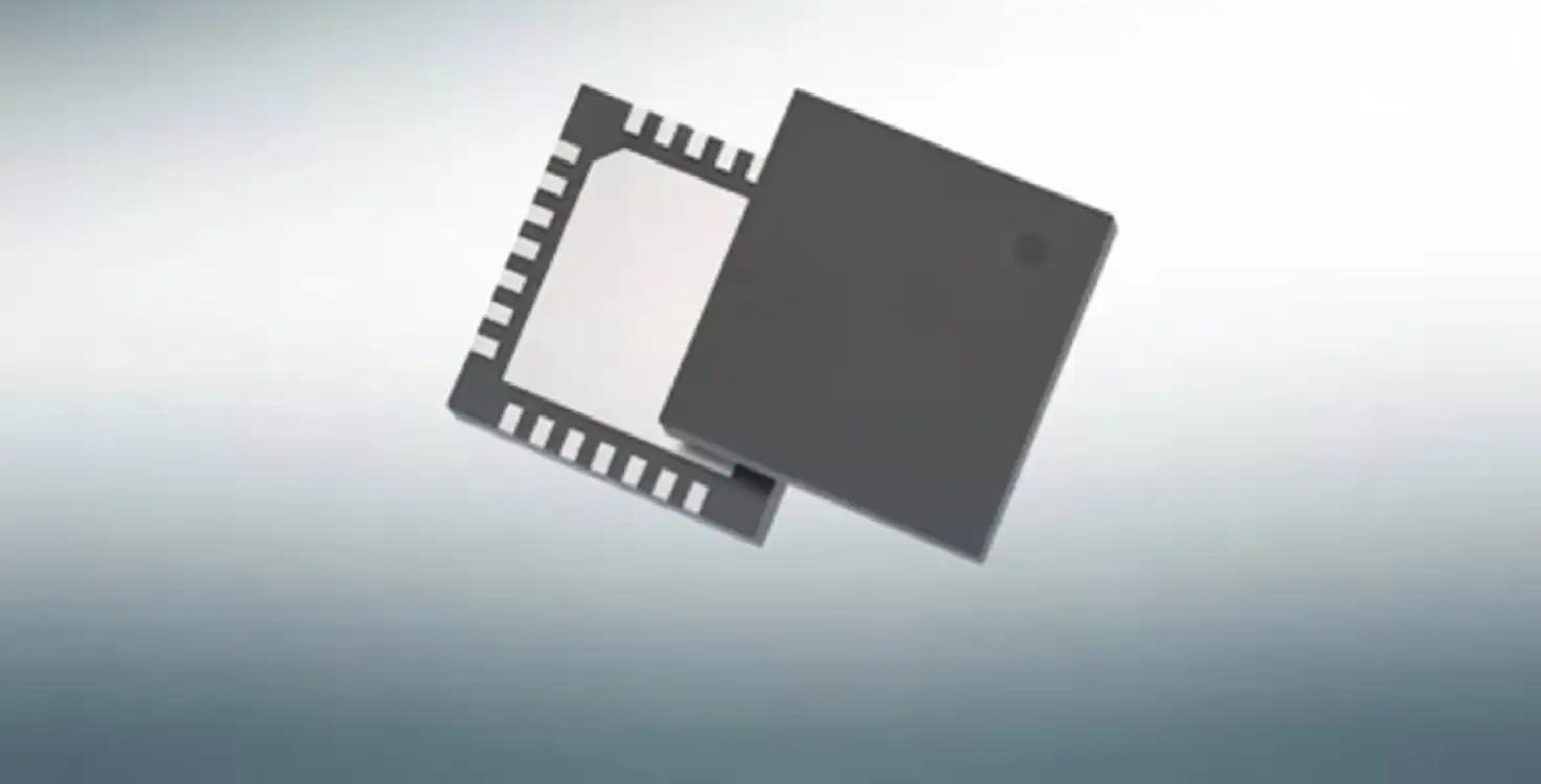
The QFN (Quad Flat No-Lead) package is a surface-mount integrated circuit package without extending leads. Instead, it uses exposed metal pads underneath the package for electrical and thermal connections. When a lid is added to the QFN, it becomes a semi-sealed or fully sealed package that offers protection and enhanced management of environmental or mechanical factors.
A QFN package with lid (sometimes referred to as a lidded QFN or open-lid/closed-lid air cavity QFN) combines the electrical efficiency of the traditional QFN design with the encapsulated protection of a plastic or metal cover. The lid can either fully seal the cavity or partially cover it depending on the application requirements.
Types of QFN Packages With Lid (2025 Classification)
As of 2025, semiconductor packaging standards classify QFN with lid configurations into three main categories:
| Configuration Type | Description | Advantages | Typical Applications |
| Lidless (Bare Die) | No lid cover; die is directly exposed. | Best thermal path; easy probing access. | RF tuning, optical alignment. |
| Flat/Partial Lid | Lid covers part of the cavity; non-hermetic. | Provides balance between thermal path and protection. | Engineering builds, testing phases. |
| Fully Lidded (Hermetic) | Complete seal using ceramic or metal lid. | Offers full environmental protection and improved reliability. | Automotive electronics, aerospace systems. |
Key Benefits of QFN Package With Lid
1. Improved Protection
Adding a lid to the QFN structure shields the exposed die from contaminants, moisture, and ESD (electrostatic discharge) damage. This is crucial in outdoor, automotive, or industrial electronic systems exposed to harsh conditions.
2. Controlled Thermal Management
The lid assists in distributing heat evenly, especially when using metal or thermally conductive materials. A lidded QFN with a heat spreader ensures temperature consistency and prevents hotspots in high-power applications.
3. Enhanced Mechanical Strength
Fully lidded packages add an extra mechanical barrier that protects delicate internal components during assembly and handling. This reduces die cracking or package warping during SMT reflow processes.
4. Compatibility With Modern Manufacturing
The QFN package with lid remains compatible with standard SMT (Surface-Mount Technology) reflow processes. Its design accommodates automated pick-and-place production lines, reducing manufacturing complexity.
5. Optimized for High Frequency & RF Performance
In 2025, advancements in 5G, EVs, and satellite systems have further proven that lidded QFNs excel in maintaining low parasitics and superior thermal dissipation, thereby supporting high-frequency and power-sensitive circuits.
Design Insights: Structure and Material Choices
Basic Structural Layers
A QFN package with lid typically includes the following components:
- Die Attach Pad (DAP) – Acts as the mechanical base and thermal conductive path.
- Lead Frame – Connects die bond pads to external terminals.
- Encapsulation Body – Provides mold compound protection (plastic or ceramic).
- Lid/Cap – Metal (e.g., copper, aluminum) or ceramic lid bonded via epoxy or solder.
Material Considerations
Choosing the right lid material impacts both reliability and thermal performance:
| Lid Material | Key Properties | Best Use Case |
| Metal (Cu, Al) | Excellent thermal conduction | Power management & RF ICs |
| Ceramic | Hermetic seal, insulation | Aerospace & defense applications |
| Plastic Mold Compound | Cost-effective, lightweight | Mass-market consumer devices |
Thermal Interface Design
The heat dissipation path for a lidded QFN is generally from the die through the die attach pad, into the PCB, and partially through the lid if thermally conductive material is used. Designers often apply thermal vias and copper planes on the PCB to enhance heat flow.
Applications of QFN Package With Lid (2025 Focus)
1. Consumer Electronics
In smartphones, tablets, and wearables, QFN with lid helps improve compactness while ensuring heat control for processors, sensors, and power ICs.
2. Automotive Electronics
Modern vehicles demand components that can endure elevated temperatures and vibrations. Lidded QFNs are found in ECUs, ADAS modules, and power converters due to their reliability and environmental resistance.
3. RF and 5G Communication Systems
According to 2025 market reports, more than three million QFN-lidded components were deployed in global 5G base stations. Their low inductance and under-1pF capacitance levels make them ideal for RF amplifiers and antennas.
4. Industrial Automation
Motor controllers, IoT control modules, and industrial sensors leverage lidded QFNs to reduce signal noise and maintain performance under continuous operation.
5. Medical and Aerospace Devices
For these safety-critical systems, hermetically lidded variants (ceramic or metal) ensure zero contamination and high reliability in extreme environments.
Design Considerations When Using QFN Packages With Lid
1. PCB Layout Recommendations
Maintain solder mask-defined pads to reduce solder bridging.
Include multiple thermal vias beneath the die area.
Ensure correct stencil thickness (typically 0.1 mm) for uniform solder application.
2. Thermal Simulation and Validation
Simulation tools like ANSYS or Cadence Allegro aid in verifying thermal performance before prototype runs. Design teams must check junction temperature under maximum load scenarios.
3. Moisture Sensitivity Level (MSL)
Fully lidded QFNs achieve better MSL ratings than lidless ones. Always follow JEDEC J-STD-020 standards for proper baking and reflow handling.
4. Lid Attachment Process Control
Improper lid attach can lead to warping or delamination. Epoxy curing and reflow profiles must match lid material properties to maintain stress balance.
Challenges and Limitations
While the QFN package with lid offers many benefits, certain limitations must be managed:
- Reduced Direct Heat Dissipation: Compared to lidless variants, thermal transfer can slightly decrease depending on lid type.
- Cost Increase: The lid add-on and sealing process increase assembly cost.
- Limited Die Access: Post-sealing tests or rework become more complex.
Thus, balancing functionality and manufacturability is essential in choosing the correct configuration for the target application.
QFN Package With Lid vs Traditional QFN Package
| Feature | QFN (Standard) | QFN Package With Lid |
| Thermal Performance | Excellent (direct die contact) | Very good, lid assists heat spread |
| Mechanical Protection | Moderate | High (protected against moisture & ESD) |
| Probing / Debug Access | Easy | Limited, lid removal may be needed |
| Cost | Lower | Slightly higher due to lid fabrication |
| Best Use Cases | R&D, low-cost consumer devices | Automotive, RF, industrial, aerospace |
Future Trends (2025–2030 Outlook)
With progress in AI hardware, EV systems, and mmWave 5G modules, QFN packages with lids are expected to evolve both in materials and structure:
- Integration with Thermal-Graphene Lids: Emerging lid designs incorporate conductive nanomaterials to double the thermal transfer efficiency.
- Hybrid Hermetic Packaging: Combining polymer-based sealing with aluminum lids to minimize cost without compromising isolation.
- Panel-Level Manufacturing: New 2025 standards allow batch process fabrication of multiple QFN-lidded units, increasing production efficiency.
- Hybrid QFN-BGA Transitions: For power semiconductors, mixed footprint designs merging QFN pad layouts and BGA thermal balls are under active development.
Conclusion
A QFN package with lid represents a significant advancement in microchip packaging technology. It balances the compactness and performance of traditional QFNs with additional protection, thermal management, and reliability benefits required by modern high-power and precision applications. As semiconductor design continues to embrace miniaturization and integration especially in industries like 5G, electric vehicles, and aerospace the lidded QFN package will remain one of the most versatile and future-ready solutions.
More Info To Visit Inter Net Chicks